
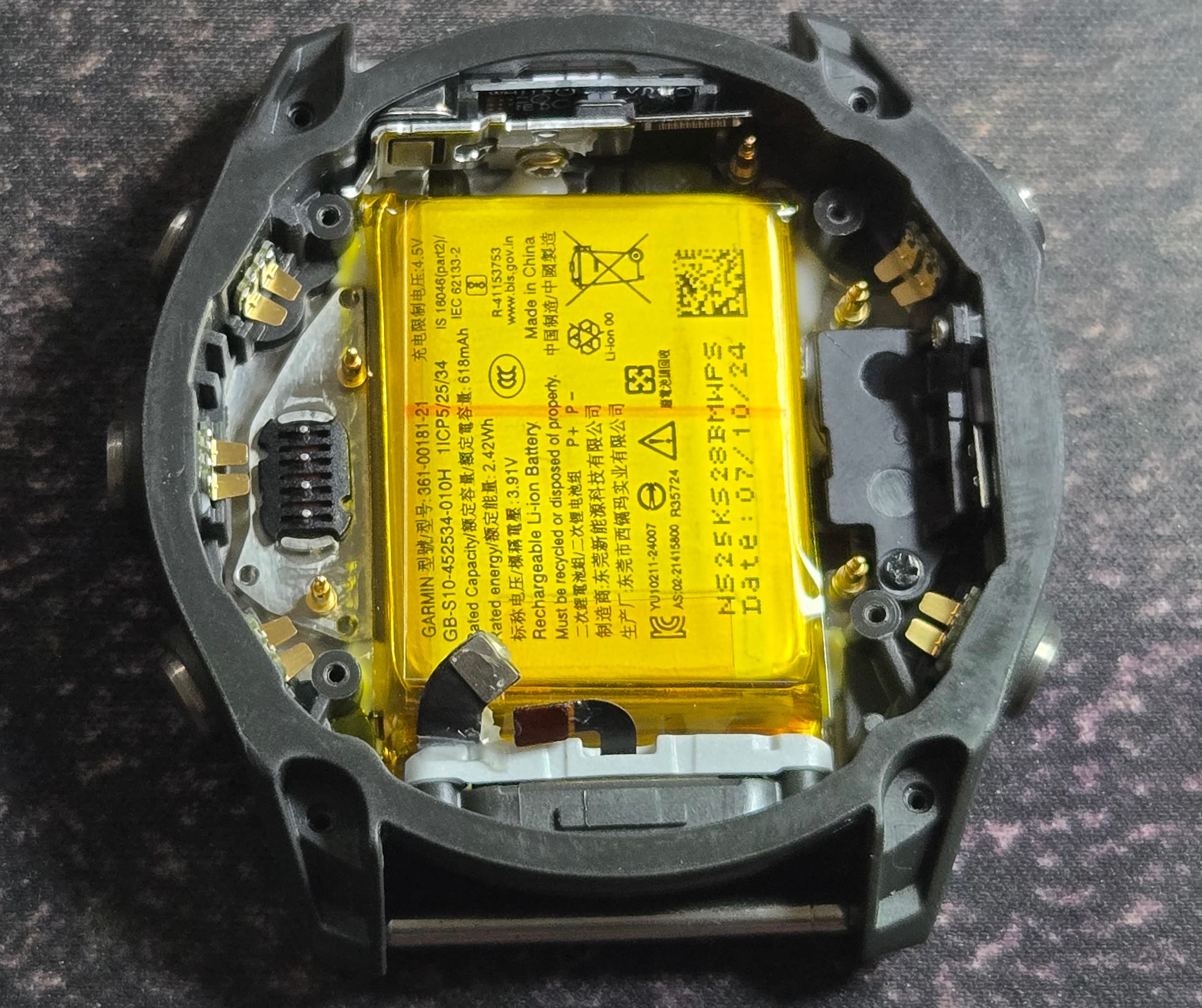
Garmin Fenix 8 TEARDOWN Details – including a new GNSS chipset
F Tipi’s Turkish blog has just detailed most of the internal components of the Fenix 8 in his detailed teardown. I only summarise and comment on the implications in this article, and you are encouraged to read the detailed original report for the techy details.
The biggest surprise to me was the change in the GNSS chipset supplier. Now that I’ve seen the details, it makes sense. Read on…
More: Garmin Fenix 8 Review
Key Takeaways
Essentially, Fenix 8 is a Fenix 7 with better dive capabilities, a speaker and a microphone.. From the outside and the official specs, we already knew that.
The display, processor, and architecture are unchanged between Fenix 7x and Fenix 8, but the battery capacity is slightly increased. Combined with a more power-efficient GNSS chipset (SYN4778), this has contributed towards improved runtime.
The architecture of the SRAM seems limited compared to other teardowns of competitor products, explaining the poor pan and zoom on maps reported on this site and elsewhere.
Technical component comparison
| Component | Garmin Fenix 8 Solar (51mm) | Garmin Fenix 7X Solar | Notes |
|---|---|---|---|
| Display | Sharp LS014B7DD01, 1.39″, 280×280, MIP | Sharp LS014B7DD01, 1.39″, 280×280, MIP | Identical reflective MIP panel |
| Main SoC (Processor) | NXP i.MX RT595 (MRT595SFF0C) | NXP i.MX RT595 (MRT595SFF0C) | Same dual-core (ARM Cortex-M33 + Cadence Fusion F1 DSP) |
| On-chip RAM | 5 MB SRAM (32 blocks, 32–256 KB each) | 5 MB SRAM (same configuration) | No external RAM used; internal SRAM powers map functionality |
| 2D GPU | Integrated in SoC, 200 MHz | Integrated in SoC, 200 MHz | Supports basic map rendering |
| Battery | 3.91V, 618mAh, 2.42Wh | 3.8V, 600mAh (Amperex) | Slight capacity increase in Fenix 8 |
| Barometer Sensor | Likely dual-sensor setup (barometer + depth gauge) | Single barometer module | Fenix 8 adds what may be an extra depth sensor |
| Microphone | MEMS mic (likely TDK), under sensor guard and LED | New | |
| Connectors (Display/Solar) | Two: one for display, one for touchscreen + solar | Two: same configuration | Identical layout |
| Flashlight Module | Present, connected via dedicated upper connector | Present | Functionally identical |
| Motherboard Spring Pins | 6 total (3 per side) | 6 total | Transfer HR and antenna signals |
| Charging/Data Chip | STMicroelectronics near USB pads | STMicroelectronics near USB pads | Same data/power interface chip |
| Waterproofing Gasket | Blue/green updated colour gasket | Blue gasket (older version) | Cosmetic/internal material change only |
| Motherboard Version | Version 5 | Likely lower (version 4 or below) | Newer board revision in Fenix 8 |
| Sensors Behind Barometer | Possibly secondary pressure or backup sensor | Single known barometer | Adds complexity to environmental sensing on the Fenix 8 |
I doubt the gasket is cosmetic. There is no reason for it to be cosmetic because it isn’t user facing. I think it’s a different material for the increased water proofing and my suspicion is that it is color coded to differentiate it. If you can get a Descent to disassemble to check if the gasket material seems to match — that would be great. 😉
I think the battery in the epix 51mm and fenix 8 51mm is the same one from the enduro 2.
The fenix barometer has plenty of room for improvement. I’m not sure if there was any improvement or not. I have still seen elevation drift over a looped course. Maybe the changes are really just about depth gauge and again if someone could disassemble a Descent to compare — cool! 🙌
The GNSS chip is also new. I met one early fenix 8 (AMOLED) adopter who is an elite trail runner and professional guide in the alps. She said the turn and off course notifications accuracy in the mountains are substantially improved and it was why she was using a fenix 8 despite the other wonky bugs back in December. I can’t speak to that myself but enecdata of one.
I think the MIP fenix 8 is not much of an upgrade from a fenix 7X. (In fact the enduro 3 seems much more fit for purpose as a MIP 51mm upgrade from the 7X.) Nor is the amoled version from a 51mm Epix 2.
‘cosmetic’ can mean that it’s just changed for no apparent reason but looks different. as opposed to improved cosmetic appearance
Ok fair enough but the choice of the word “cosmetic” has a meaning that it is an aesthetic rather than functional change. I was dubious it is an aesthetic choice rather than either a side effect of a materials change or a color coding that is meaningful in the supply chain or factory or both.
Agree wth Brian. Cosmetic is not quite the correct term here. If anything the change in visual appearance is inconsequential to the user.
No wonder maps are so slow, 5mb of ram in 2025. What the hell!
Compare the garmin ones to coros or workoutdoors on the AW
Thanks for the summary, Ferhad Fidan done a good job as usual.
Every Series embedded the same CPU since 2021, that’s said we cannot understand the strategy of Garmin with the “System” base OS.
I find the findings interesting but not surprising. Seems a lot of “updates” especially in Garmin town are code rather than hardware. It would also explain why most new Garmin Fenix products can be so buggy.
yep
my fr965 had the triangle of death a couple of times last week in the gym
it’s completely unacceptable, imho, that a 2-year old watch does this
Agreed. My Fenix 7x has a restart bug where if I turn if off it automatically restarts. Power spikes up to and over 1000 watts which is no where near accurate and elevation is no longer trackable.
Beta and off beta does not fix these issues except the restart issue. My apex 2 pro is the same age and keeps chugging along.